
What is the FPGA?
An integrated circuit known as a field programmable gate array (FPGA) comprises of internal hardware blocks with user-programmable interconnects to tailor operation for a particular purpose. The interconnects are easily reprogrammable, enabling an FPGA to enable a new application or accept design modifications over the course of the part’s lifetime.

When compared to ASIC technologies with fixed functions, like conventional cells, FPGAs can offer a variety of benefits. ASICs typically take months to create and cost thousands of dollars to purchase the device. However, FPGAs may be made in less than a second, and they can cost anything from a few dollars to a few thousand. The FPGA’s flexibility has a hefty price tag in terms of space, power, and delay. An FPGA uses 20 to 35 times more space than a conventional cell ASIC while performing at speeds that are 3 to 4 times slower. This article discusses the fundamentals of FPGAs and the switch matrix, logic blocks, and I/O pad of the FPGA architecture module. If you want to learn more information about FPGA series such as Zynq-7000 SoC, FPGA Spartan-7, or Virtex-7 FPGAs, you can visit Vemeko FPGA website to learn more detailed information about them.
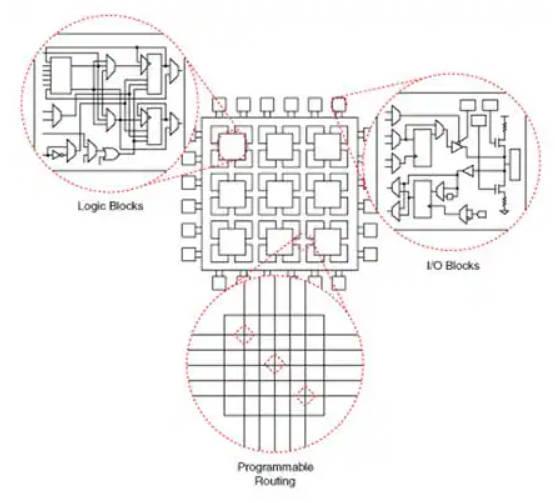
FPGA Architecture
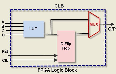
The CLB may alternatively be referred to as a logic block (LB), a logic element (LE), or a logic cell (LC), depending on the manufacturer. The MUX (Multiplexer), D flip-flop, and LUT components of a logic block. The MUX is utilized for selection logic, the LUT performs the combinational logical operations, and the D flip flop stores the LUT’s output. The Look Up Table-based function generator is the fundamental component of the FPGA. Following tests, the LUT can have 3, 4, 6, or even 8 inputs. We now have adaptive LUTs, which use two function generators to implement two outputs from a single LUT.
The most well-known FPGA, the Xilinx Virtex-5, has a flip-flop and a look-up table (LUT) that are coupled by MUX. Thousands or hundreds of customizable logic blocks make up the modern FPGA. Modelsim and Xilinx ISE software are used for development and to create a bitstream file for setting the FPGA.
CPLD vs. FPGA
Low power consumption, low logic density, and minimal complexity per chip are the main features of entry-level FPGAs. Functional blocks with specialized functions are added by devices with higher functionality: Phase-locked loops (PLLs), high-speed serializers and deserializers, Ethernet MACs, PCI express controllers, and high-speed transceivers are a few examples. These blocks can either be created as independent circuits, which is hard IP, or implemented with CLBs, which is referred to as soft IP. Performance is increased with hard IP blocks at the expense of reconfigurability. At the top end, the FPGA product family includes sophisticated system-on-chip (SoC) components that combine a microprocessor CPU core, hard IP, and the FPGA architecture into a single device. A SoC FPGA offers greater integration, lower power consumption, a smaller board footprint, and higher-bandwidth communication between the core and additional blocks when compared to standalone devices. CPLDs and FPGAs vary primarily in that CPLDs do not modify their configuration while running. In contrast to FPGAs, which can be expanded or modified at runtime, they have a fixed functionality over time. The fundamental idea behind a CPLD is that all of the logic operations are implemented in the logic gates.
| FPGA | CPLD |
|---|---|
| FPGA has a larger power usage. | In contrast, CPLD has lower power consumption. |
| Complex apps are a good fit for FPGA. | In contrast, simpler programs work better with CPLD. |
| Up to 100,000 tiny logic blocks can be found in FPGAs. | CPLDs, in comparison, can only hold a small number of thousand logic blocks. |
| An FPGA, on the other hand, is an integrated circuit that is primarily made to be altered by a customer or a developer after production. | An integrated circuit called a CPLD aids in the operation of digital systems. |
| Compared to FPGAs, CPLD delays are far more predictable. | Because it has nonvolatile memory, CPLD is given greater protection than FPGA. |
| FPGA falls under the fine grain category. | CPLD, on the other hand, is coarse grain. |
| FPGA is similar to a Gate array. | However, the CPLD is equivalent to the PAL. |
| Performance-wise, FPGA offers dependable performance that is unaffected by internal routing. | On the other hand, CPLD’s performance is erratic and is depending on routing. |
| In contrast, FPGA is an abbreviation for Field Programmable Gate Arrays. | CPLD is an abbreviation for Complex Programmable Logic Devices. |
| A digital logic chip called an FPGA is built on RAM. | CPLDs, on the other hand, are EEPROM-based. |
Overview of SoC FPGAs
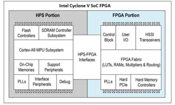
To accommodate a variety of applications, SoC FPGAs offer a wide range of processing capabilities. High-volume applications including protocol bridging, video processing cards, mobile devices, and industrial motor control drives are the focus of low-cost, low-power SoC FPGAs like Intel’s Cyclone V. The FPGA section of the device and a hard processor system (HPS) built around a single- or dual-core 32-bit Arm Cortex-A9 MPCORE operating at 925 MHz make up its two separate components. Each component has a unique collection of peripherals, including hard IP from outside vendors.
FPGA Design
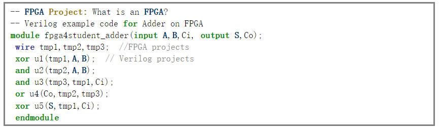
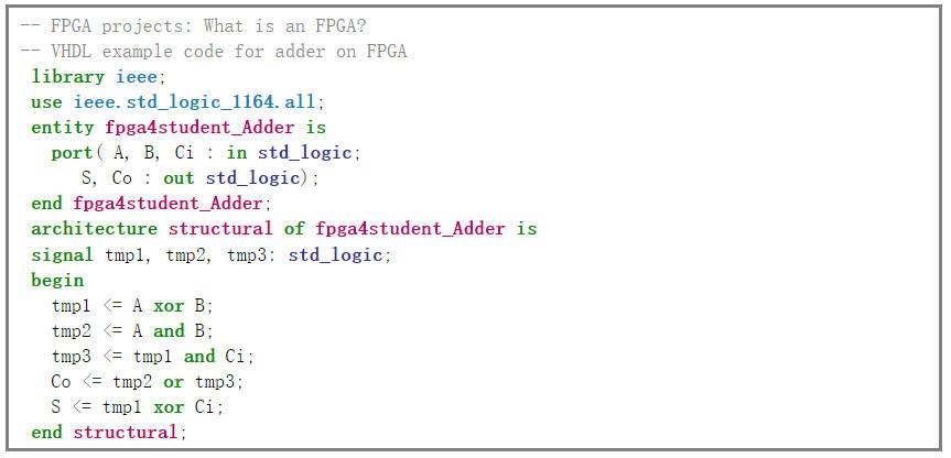
How do we create the right configuration to run the application using this collection of thousands of hardware blocks? In order to create an FPGA-based design, the necessary computing jobs must first be defined in the development tool before being combined into a configuration file that specifies how to connect the CLBs and other modules. The procedure resembles a software development cycle, but instead of creating a set of instructions to run on a predetermined hardware platform, the objective is to construct the hardware itself. To create an FPGA setup, designers have historically used a hardware description language (HDL) like VHDL or Verilog.
The fact that designing an FPGA requires both coding competence and in-depth understanding of the underlying hardware presents a barrier with an HDL approach because the necessary knowledge is not readily accessible.
Vendors are now providing software development kits (SDKs), which enable designers to create FPGA solutions in well-liked high-level languages like C/C++, Python, and OpenCL. There are also high-level synthesis (HLS) design tools that use graphical block diagrams rather than lines of code and run on platforms like National Instruments’ LabVIEW.
FPGA Applications
The ability to configure the FPGA’s CLBs into hundreds or thousands of identical processing blocks has applications in image processing, artificial intelligence (AI), data center hardware accelerators, enterprise networking, and automotive advanced driver assistance systems (ADAS). Many applications rely on the parallel execution of identical operations. Numerous of these application areas are undergoing rapid change as new protocols and standards are implemented and needs change. Manufacturers can implement systems that can be changed as needed thanks to FPGAs.
High-speed search is a great use for FPGAs: Microsoft uses FPGAs in its data centers to power the Bing search engines. New algorithms can be supported as they are developed by the FPGA through changes. The design can be adapted to execute simulation or modeling procedures in an HPC application if requirements change. An ASIC makes it difficult or impossible to achieve this flexibility. Other applications for FPGAs include wireless communications, medical electronics, consumer electronics, digital television, industrial motor control, and aerospace and defense.