
Overview of FPGA
The phrase “field-programmable” refers to an integrated circuit that can be customized by a client or a designer after production. This is known as a field-programmable gate array (FPGA). We constantly discuss the various FPGA applications and uses, but we acknowledge that we rarely discuss another subject: what exactly is an FPGA board and what is an FPGA used for?
FPGAs were created in the middle of the 1980s with the intention of enabling designers to develop unique digital logic. By the early 1990s, networking and telecommunications were the main applications for FPGAs. FPGAs which belong to Embedded IC were being employed in consumer, automotive, and industrial applications by the end of the 1990s.

How does FPGA work?
An FPGA is made up of internal hardware blocks that can have their interconnects programmed by the user to operate in a particular way for a given application. Because these interconnects are reprogrammable, the FPGA can accept design modifications or support new applications during the part’s lifespan. Although the FPGA is initially programmed during production, it can be updated to reflect any modifications made to the device. A matrix of customizable logic blocks (CLBs) coupled by programmable interconnects serves as the foundation of an FPGA. The fundamental FPGA cell is made up of CLBs, which also comprise programmable routing controllers (multiplexers), two 16-bit function generators, one 8-bit function generator, two registers (flip-flops or latches), and two registers. Macros and other designed functions are implemented using CLBs.
Different processing operations do not compete for the same resources since, unlike microprocessors, FPGAs are able to perform simultaneous operations. Each separate task is given its own area of the chip and is free to operate independently of other logic blocks. As a result, adding more activities has no impact on how well one aspect of the application performs. The internal configuration of the FPGA is set by software, or “firmware,” as it is sometimes referred to. In the event that the functionality or application needs change, FPGAs can be reprogrammed on the spot.
Verilog HDL or VHDL are two examples of Hardware Description Language that can be used to program FPGAs. FPGAs differ from ASIC ICs, which are created to perform particularly designated jobs, in that they are reprogrammable. Early on in the design process, it must be decided whether an FPGA-based design should be adopted. If the chip needs to be reprogrammed later on in the design process or even after manufacture, that should be taken into account. When flaws may still be discovered early in the development cycle, manufacturers will occasionally choose an FPGA-based design, switching to an ASIC after the design is reliable.
FPGA Features
⦁ Parallel processing: A FPGA may perform parallel processing since it does not adhere to the processor programming model. Because of parallel processing, customers can still achieve the required throughputs while using lower energy clocks (as opposed to high frequency clocks on processors).
⦁ FPGAs can be reconfigured: As a product evolves, feature changes or improvements can be easily made in the field by simply updating the FPGA.
⦁ Low and medium volume production: FPGAs are primarily utilized for low- to medium-volume devices. ASICs are often favoured in high volume items because to their reduced cost. ASICs are often more cost-effective for big volume items than for low or medium volumes.
⦁ Rapid development process: FPGAs are able to provide a quick turnaround from concept to production because actual transistor-level design is not required.
FPGA Structures
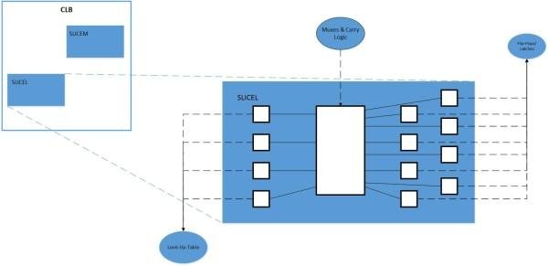
Configurable Logic Block
The fundamental piece of logic in an FPGA are configurable logic blocks (CLBs). The FPGA may accept many hardware configurations thanks to a CLB. Virtually every logic operation can be performed by CLBs with programming. Look-up tables (LUTs) and flip-flops are among the discrete logic elements found in each individual CLB.
DSP Slices
A DSP slice, also known as a block or cell in some contexts, is one of the specialized parts of an FPGA. It is more effective than employing numerous CLBs for digital signal processing tasks like filtering or multiplying. This multiplier circuitry reduces the need for flip-flops and LUTs in applications involving math and signal processing.
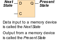
Flip-Flops
A flip-flop is a circuit that can be used to store state data and has two stable states. In an FPGA circuit, flip-flops are binary shift registers that synchronize logic and store logical states between clock cycles. A flip-flop only stores one bit of information.
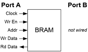
Block RAM
Block RAM, or BRAM, is the name given to the memory that can be found on an FPGA device. To create BRAM in smaller or bigger sizes, these blocks can be divided or cascaded. Algorithms for digital signal processing commonly require to maintain a whole block of data while operating without onboard memory. The programmable logic of an FPGA device does not fit all processing tasks.
Transceivers
High-speed serial data transmission and reception to and from the FPGA are made possible by the use of transceivers. High-speed data transfer can be implemented with the help of this specific component without using up FPGA logic resources.
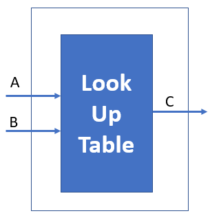
Lookup Tables
A lookup table (LUT) establishes the output for each given input or set of inputs. It is the truth table in the context of combinational logic and establishes how combinatorial logic functions. A truth table is a collection of outputs that have been predetermined for each set of inputs. When the chip is powered on, a unique truth table is stored into the LUT.
Input/Output Blocks
Data enters and exits the FPGA through input output (IO) blocks, which are parts of the system. Depending on the type of data, the IO blocks can be configured in a variety of ways. Despite moving at slower rates than transceivers, they are more functionally flexible.
FPGA Applications
So what is the purpose of an FPGA? There are numerous applications for FPGAs. Digital signal processing, biomedical instrumentation, device controllers, software-defined radio, random logic, medical imaging, computer hardware emulation, voice recognition, cryptography, filtering and communication encoding, and other specific applications using an FPGA are just a few examples. Smartphones, self-driving cars, cameras, displays, video and image processing, and security systems are examples of consumer electronics applications. The benefits of FPGAs are also used in many commercial applications, including as servers and a variety of industries like aerospace and defense, medical electronics, and distributed financial systems.
Advantages of FPGA
Performance: When compared to other contemporary microprocessors, FPGAs offer superior performance in terms of processing power, speeds, reaction times, and overall performance due to their parallel nature.
Reprogrammable hardware structure: FPGAs’ re-programmability allows functionality to be changed even after they are manufactured. After the product has been put in the field, users can program additional features and functionalities, conform to new standards, and change hardware applications.
Quicker time to market: Users can create systems based on this technology quickly because to the availability of FPGAs. ASICs require multi-month manufacturing cycles. Users of FPGAs can start shipping systems as soon as a product design is tested and functional.
Lower overall costs: FPGAs are reasonably priced when compared to the expense of producing an ASIC. An ASIC has a lengthy design cycle, and the production equipment is expensive. Additionally, a new chip will be needed if the design is changed, as opposed to an FPGA, which can simply be updated with a new program.
Low maintenance: FPGAs, as opposed to ASICs, can be upgraded or improved on-the-fly without requiring the time and resources needed to modify circuit boards and hardware. In comparison to ASICs, engineering expenditures are also significantly lower. System needs might vary over time, and updating an FPGA incrementally is cheaper than retooling for an ASIC, which can be very expensive.