
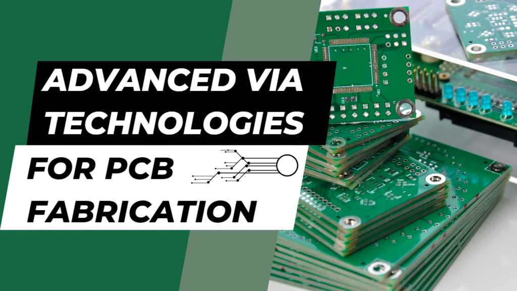
Printed circuit boards (PCBs) have come a long way since their discovery, and with refinements in technology, there is a constant demand for PCBs to be smaller, faster, and more efficient. One of the ways manufacturers achieve these is by advanced via technologies such as blind, buried, and micro vias. In this article, we’ll explore these technologies and their importance in modern PCB fabrication.

Blind Vias
Blind vias are used to connect the outer layer of a PCB to one or more inner layers without penetrating the entire board. They are called “blind” because they are visible from one side of the PCB but not the other. Blind vias allow for high-density interconnections between the outer layers of a PCB and the inner layers, without the need for multiple layers of wiring. Blind vias are especially useful in designs where space is at a premium, as they allow for more routing space on the outer layers of the board.
Buried Vias
Buried vias are used to one or multiple layers of a PCB without penetrating the outer layer. They are called “buried” because they are not visible from either side of the PCB. Buried vias are useful in designs where space is limited, as they allow for more routing space on the outer layers of the board. Buried vias are also useful in high-speed designs, as they can reduce the amount of inductance and capacitance in the circuit.
Micro Vias
Micro vias are used to connect the outer layers of a PCB to the inner layers with a diameter of less than 0.15mm. They are useful in designs where space is at a premium, as they allow for more routing space on the outer layers of the board. Micro vias are also useful in high-speed designs, as they can reduce the amount of inductance and capacitance in the circuit.
Benefits of Advanced Via Technologies
Advanced via technologies such as blind, buried, and micro vias offer several benefits in modern PCB fabrication. These benefits include:
Increased Density Advanced via technologies allow for higher density PCB designs, with more connections per unit area.
Improved Signal Integrity Advanced via technologies reduce the inductance and capacitance amounts in the circuit, improving signal integrity and reducing noise.
More Routing Space Advanced via technologies allow for more routing space on the outer layers of the PCB, making it easier to route complex designs.
Reduced Cost Advanced via technologies can reduce the number of layers required in a PCB design, reducing the cost of manufacturing.
Increased Flexibility Advanced via technologies allow for more flexibility in PCB design, making it easier to design complex circuits with multiple layers.
Conclusion
In conclusion, advanced via technologies such as blind, buried, and micro vias are critical components in modern PCB fabrication. They offer several benefits, including increased density, improved signal integrity, more routing space, reduced cost, and increased flexibility. These advancements have made it possible to design smaller, faster, and more efficient PCBs. When designing a PCB with advanced via technologies, it’s essential to choose a reliable and experienced PCB manufacturing service provider such as ELE PCB.