
Step 1 – The Design – PCBWay
Circuit boards should be rigorously compatible with, a PCB layout created by the designer using PCB design software. Commonly-used PCB design software includes Altium Designer, OrCAD, Pads, KiCad, Eagle, etc. NOTE: Before PCB fabrication, designers should inform their contract manufacturer about the PCB design software version used to design the circuit since it helps avoid issues caused by discrepancies.
Once the PCB design is approved for production, designers export the design into a format of their manufacturer’s support. The most frequently used program is called extended Gerber. Gerber also goes by the name IX274X.
The PCB industry birthed extended Gerber as the perfect output format. Different PCB design software possibly calls for different Gerber file generation steps, they all encode comprehensive vital information including copper tracking layers, drill drawing, apertures, component notations, and other options. All aspects of the PCB design undergo checks at this point. The software performs oversight algorithms on the design to ensure that no errors go undetected. Designers also examine the plan with regard to elements relating to track width, board edge spacing, trace and hole spacing, and hole size.
After a thorough examination, designers forward PCB files to PC Board Houses for production. To ensure the design fulfills requirements for the minimum tolerances during the manufacturing process, almost all PCB Fab Houses run Design for Manufacture (DFM) check before circuit boards fabrication.

Step 2 – Printing the Design
A special printer called a plotted printer is used to print the design of the PCB. It produces a film that shows the details and layers of the board. When printed, there will be two ink colors used on the inside layer of the board:
- Clear Ink to show the non-conductive areas; and
- Black Ink to show the conductive copper traces and circuits.
The same colors are used for the outer layers, but the meaning of them is reversed.
Step 3 – Creating the Substrate
Now is when the PCB will start to form. The substrate, which is the insulating material (epoxy resin and glass fiber) that holds the components on the structure, begins forming by passing the materials through an oven to be semicured. Copper is pre-bonded to both sides of the layer and then etched away to show the design from the printed films.
Step 4 – Printing the Inner Layers
Stage 1 is to transfer the image using an artwork film to the board surface, using photosensitive dry-film and UV light, which will polymerise the dry film exposed by the artwork. This step of the process is performed in a clean room.<br> Imaging – The process of transferring electronic data to the photo-plotter, which in turn uses light to transfer a negative image circuitry pattern onto the panel or film.


Step 5 – Ultraviolet Light
Once aligned, the resist and laminate go under ultraviolet lights to harden the photoresist. The light reveals the pathways of copper. The black ink from before prevents hardening in areas that will be removed later on. The board is then washed in an alkaline solution to remove the excess photoresist.
Step 6 – Removing Unwanted Copper
Now, it is time to remove any unwanted copper that remained on the board. A chemical solution, similar to the alkaline solution, eats away at the unwanted copper. The hardened photoresist remains intact.
Step 7 – Inspection
The newly-cleaned layers will need to be inspected for alignment. The holes drilled earlier help align the inner and outer layers. An optical punch machine drills a pin through the holes to keep the layers lined up. After the optical punch, another machine will inspect the board to ensure there are no defects. From here on out, you will not be able to correct any missed errors.
Step 8 – Laminating the Layers
Now, you will see the board take shape as the layers are fused together. Metal clamps hold the layers together as the laminating process begins. A prepreg (epoxy resin) layer goes on the alignment basin. Then, a layer of substrate goes over the prepreg followed by a copper foil layer and more prepreg resin. Lastly, there is on more copper layer applied, which is the press plate.
Step 9 – Pressing the Layers
A mechanical press is then used to press the layers together. Pins are punch through the layers to keep them properly aligned and secured, these pins can be removed depending on the technology. If correct, the PCB will go to the laminating press, which applies heat and pressure to the layers. The epoxy melts inside of the prepreg that, along with the pressure, fuses the layers together.
Step 10 – Drilling
The components that have to be attached to the multi-layered PCB can be done only by VIAS drilling. That is, a pated-through hole is drilled in the shape of annular rings. Small drill bits that are made out of tungsten carbide is used for the drilling. A dremel drill press is normally used to punch the holes. Usually, a 0.035 inch drill bit is used. For high volume production automated drilling machines are used.

Sometimes, very small holes may have to be drilled, and mechanical methods may permanently damage the PCB. In such cases, laser-drilled VIAS may be used to produce an interior surface finish inside the holes.
The board is now ready to be plated. A chemical solution fuses all of the layers together. The board is then thoroughly cleaned by another series of chemicals. These chemicals also coat the panel with a thin copper layer, which will seep into the drilled holes.
Step 11 – Plating
The board is now ready to be plated. A chemical solution fuses all of the layers together. The board is then thoroughly cleaned by another series of chemicals. These chemicals also coat the panel with a thin copper layer, which will seep into the drilled holes.


Step 12 – Outer Layer Imaging
Similar to the inner layer process (image transfer using photosensitive dry film, exposure to UV light and etching), but with one main difference – we will remove the dry film where we want to keep the copper/define circuitry – so we can plate additional copper later in the process.
This step of the process is performed in a clean room.

Step 13 – Plating
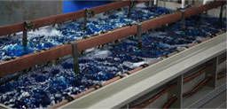
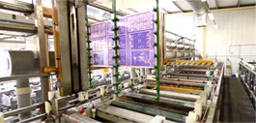
Second electrolytic plating stage, where the additional plating is deposited in areas without dry film (circuitry). Once the copper has been plated, tin is applied to protect the plated copper.


Step 14 – Etching
The same chemical solution from before removes any unwanted copper under the resist layer. The tin guard layer protects the needed copper. This step established the PCB’s connections.


Step 15 – Solder Mask Application
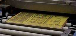
Before the solder mask is applied to both sides of the board, the panels are cleaned and covered with an epoxy solder mask ink. The boards receive a blast of UV light, which passes through a solder mask photo film. The covered portions remain unhardened and will undergo removal.
Finally, the board passes into an oven to cure the solder mask.
Step 16 – Silkscreening
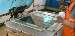
It is often necessary to print text and place other small printed idents onto a PCB. This can help in identifying the board, and also in marking component locations to aid in fault finding, etc. A silk screen generated by the PCB design software is used to add the markings to the board, after the other manufacturing processes for the bare board have been completed.
Step 17 – Surface Finish
To add extra solder-ability to the PCB, we chemically plate them with gold or silver. Some PCBs also receive hot air-leveled pads during this stage. The hot air leveling results in uniform pads. That process leads to the generation of surface finish.


Step 18 – Profile
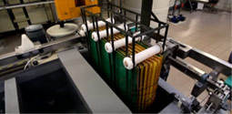
This is the process of cutting the manufac-turing panels into specific sizes and shapes based upon the customer design as defined within the gerber data. There are 3 main options available when providing the array or selling panel – scoring, routing or punching. All dimensions are measured against the customer supplied drawing to ensure the panel is dimensionally correct.
Step 19 – Electrical test
Used for checking the integrity of the tracks and the through-hole interconnections – checking to ensure there are no open circuits or no short circuits on the finished board. There are two test methods, flying probe for smaller volumes and fixtures based on volumes.

Step 20 – Final inspection
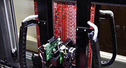
In the last step of the process, a team of sharp-eyed inspectors gives each PCB a final careful check-over. Visual checking the PCB against acceptance criteria and using PCBWay “approved” inspectors. Using manual visual inspection and AVI – compares PCB to Gerber and has a faster-checking speed that human eyes, but still requires human verification.


